The rapid growth of the electronics industry has increased the demand for reliable and efficient manufacturing processes. From smartphones and computers to medical equipment and industrial automation systems, virtually every electronic product depends on a printed circuit board (PCB). However, creating a functional electronic device involves more than simply producing a circuit board. The complete manufacturing process includes both PCB fabrication and component assembly, commonly referred to as PCB Print and Assembly.
PCB Print and Assembly combines the production of the printed circuit board with the installation of electronic components to create a fully functional electronic assembly. This integrated process helps manufacturers streamline production, improve quality control, and accelerate product development. Understanding PCB Print and Assembly is essential for engineers, product developers, and businesses involved in electronics manufacturing.
What Is PCB Print and Assembly?
PCB Print and Assembly refers to the complete process of manufacturing a printed circuit board and assembling electronic components onto it. The process begins with PCB fabrication, where conductive pathways are created on a non-conductive substrate. Once the board is manufactured, electronic components are mounted and soldered to create a functional circuit.
The term combines two critical stages of electronics production:
- PCB printing or fabrication
- PCB assembly
Together, these processes transform design files into fully operational electronic products ready for testing and deployment.
Many manufacturers offer PCB Print and Assembly as a turnkey solution, simplifying project management and reducing supply chain complexity for customers.
Importance of PCB Print and Assembly
Modern electronic devices require highly reliable circuit boards capable of supporting increasingly complex functions. The quality of both fabrication and assembly directly impacts product performance, durability, and reliability.
A well-executed PCB Print and Assembly process provides several benefits:
- Improved manufacturing efficiency
- Reduced production lead times
- Better quality control
- Simplified supplier management
- Lower overall production costs
- Faster product development cycles
By integrating fabrication and assembly under one manufacturing partner, companies can reduce communication challenges and improve production consistency.
The PCB Printing Process
The first stage of PCB Print and Assembly involves manufacturing the printed circuit board itself.
The process begins with PCB design files that define circuit layouts, copper traces, vias, component locations, and board dimensions.
Manufacturers then create the PCB using a series of fabrication steps.
Copper-clad laminate materials serve as the base substrate. Circuit patterns are transferred onto the copper layers using imaging technologies, followed by chemical etching to remove unwanted copper.
After etching, holes are drilled for vias and component mounting locations. Copper plating is applied to establish electrical connections between layers.
Additional processes such as solder mask application, silkscreen printing, and surface finishing complete the board fabrication stage.
The result is a bare PCB ready for component assembly.
PCB Design Considerations
Successful PCB Print and Assembly begins with effective PCB design.
Engineers must consider several factors when creating a circuit board layout.
These include:
- Component placement
- Signal routing
- Power distribution
- Thermal management
- Electromagnetic compatibility
- Manufacturability requirements
Proper design practices help ensure reliable performance while minimizing assembly challenges and production costs.
Design for Manufacturability (DFM) principles are commonly used to optimize designs for efficient fabrication and assembly.
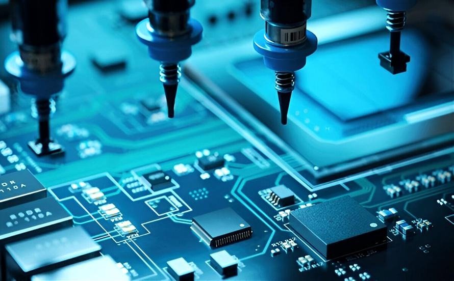
The PCB Assembly Process
Once fabrication is complete, the PCB moves to the assembly stage.
PCB Print and Assembly includes mounting electronic components onto the board and creating permanent electrical connections.
The assembly process typically begins with solder paste application. A precision stencil deposits solder paste onto designated component pads.
Automated pick-and-place machines then position components according to assembly specifications.
These machines can place thousands of components per hour with exceptional accuracy.
After placement, soldering processes permanently attach components to the board and establish electrical connections.
Surface Mount Technology in PCB Print and Assembly
Surface Mount Technology (SMT) is the most common assembly method used in modern electronics manufacturing.
SMT components are mounted directly onto the surface of the PCB rather than inserted through holes.
Advantages of SMT include:
- High assembly speed
- Smaller component sizes
- Increased circuit density
- Lower manufacturing costs
- Improved automation
Most consumer electronics and advanced electronic products rely heavily on SMT assembly techniques.
SMT supports the miniaturization trends that continue to drive innovation throughout the electronics industry.
Through-Hole Assembly
Although SMT dominates modern production, Through-Hole Technology (THT) remains important for many applications.
Through-hole components feature leads that pass through drilled holes in the PCB and are soldered on the opposite side.
This assembly method provides strong mechanical connections and is commonly used for:
- Connectors
- Transformers
- Power components
- Relays
- Heavy-duty electronic assemblies
Many products combine SMT and THT components within a single assembly.
PCB Print and Assembly providers must often support both technologies to meet customer requirements.
Quality Control in PCB Print and Assembly
Quality assurance is critical throughout the entire manufacturing process.
Manufacturers use multiple inspection and testing methods to verify assembly quality and functionality.
Automated Optical Inspection (AOI) systems analyze component placement, solder joints, and assembly accuracy.
X-ray inspection allows engineers to examine hidden solder joints beneath advanced component packages such as Ball Grid Arrays (BGAs).
Electrical testing verifies circuit operation and identifies defects that may not be visible through physical inspection.
Comprehensive quality control procedures help reduce defect rates and improve product reliability.
Factors Affecting PCB Print and Assembly Costs
Several factors influence manufacturing costs.
Board complexity is one of the most significant cost drivers. Multilayer boards, high-density designs, and advanced materials generally increase fabrication expenses.
Component count and package complexity also affect assembly costs.
Additional factors include:
- Production volume
- Material selection
- Testing requirements
- Lead time expectations
- Assembly technology
Understanding these factors helps businesses make informed manufacturing decisions and optimize production budgets.
Applications of PCB Print and Assembly
PCB Print and Assembly supports virtually every segment of the electronics industry.
Consumer electronics manufacturers use assembled PCBs in smartphones, tablets, wearable devices, gaming systems, and smart home products.
Medical equipment relies on high-reliability circuit boards for patient monitoring systems, diagnostic instruments, and imaging devices.
Automotive manufacturers incorporate assembled PCBs into engine control units, infotainment systems, safety technologies, and electric vehicle electronics.
Industrial automation systems use PCB assemblies in robotics, controllers, sensors, and monitoring equipment.
Telecommunications, aerospace, defense, renewable energy, and IoT applications also depend heavily on advanced PCB manufacturing processes.
Future Trends in PCB Print and Assembly
The electronics industry continues to evolve rapidly, driving innovation in PCB manufacturing and assembly technologies.
Emerging trends include:
- High-density interconnect (HDI) boards
- Flexible and rigid-flex circuits
- Advanced semiconductor packaging
- Artificial intelligence-driven manufacturing
- Smart factory automation
- Lead-free production processes
Manufacturers are investing in advanced equipment and digital technologies to improve quality, efficiency, and sustainability.
As electronic products become increasingly complex, integrated PCB Print and Assembly services will continue to play a vital role in supporting innovation and market growth.
Conclusion
PCB Print and Assembly is a comprehensive manufacturing process that combines PCB fabrication with component assembly to create fully functional electronic products. By integrating these critical production stages, manufacturers can improve efficiency, enhance quality control, reduce lead times, and simplify supply chain management. From consumer electronics and medical devices to automotive systems and industrial automation equipment, PCB Print and Assembly supports a wide range of applications across modern industries. As technology continues to advance, companies that partner with experienced manufacturing providers can benefit from reliable production, consistent quality, and scalable solutions for everything from prototype development to high-volume production, including specialized applications such as Inverter PCB Assembly.